Introduction
This is the first in a series of posts about programming the Nintendo Entertainment System (NES) game console. Released more than 35 years ago, the NES represents a way of programming that I have no experience of. Like most developers, I program in high-level languages that hide the underlying CPU architecture. In contrast, NES programs are often 'hand crafted' in assembly to get the best out of the limited hardware. This involves learning about opcodes, addressing modes, registers, the call stack, interrupts, and more. This truly is bare metal programming! But before that, I want to start with an overview of the console.
The NES
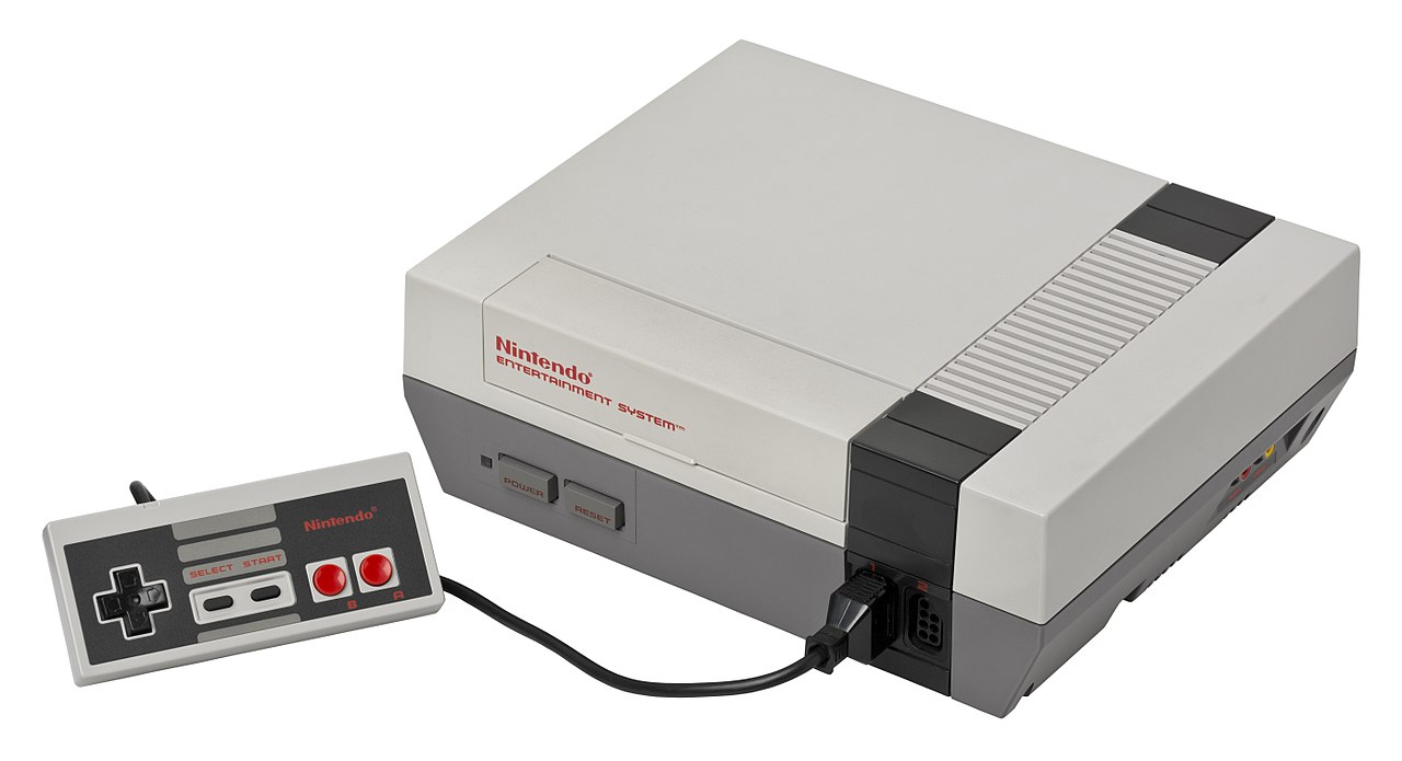
Nintendo released the NES in the West in the mid 80s. It was the export version of the Famicom, Nintendo's home console that they released in Japan in 1983. Games were sold on cartridges called Game Paks that plugged into the console. It came with two game controllers. Each controller has a D-pad, A and B action buttons, a Start button, and a Select button. The console itself has only two buttons: Power and Reset.
There was a version of the NES for the PAL colour television standard and another for the NTSC standard. The console was a hit and Nintendo then developed two arcade versions of the NES: the Nintendo VS. System and the PlayChoice-10. They also made various peripherals, including alternative controllers such as the Zapper. By the mid 90s Nintendo had released the Super NES and sales of the NES had dropped. Nintendo discontinued the NES in 1995.
The CPU
At the heart of the NES is a central processing unit (CPU) made by Ricoh. This is based on the MOS Technology 6502 but it omits a patented binary coded decimal mode. The NTSC NES and the PAL NES use different versions of the Ricoh CPU. The former uses the Ricoh 2A03 (a.k.a. RP2A03) and the latter uses the Ricoh 2A07 (a.k.a. RP2A07).
A CPU works by executing machine instructions. Each instruction starts with an instruction operation code (opcode). The opcode identifies the particular operation that the CPU should perform. The 6502 has 151 official opcodes. Many of them include information — an operand — that identifies the data to be operated on.
The clock rate determines the speed at which a CPU can execute instructions. It is measured in clock cycles per second. The clock rate of the NES's CPU depends on the version of the console. The PAL version has a clock rate of 1.66 MHz and the NTSC version has a clock rate of 1.79 MHz. Most instructions take from 2 to 7 clock cycles to execute.
Code written in the form of machine instructions is called machine code. Games for the NES are usually written in assembly. This is a low-level programming language that resembles machine code but is easier to write. An assembler is used to convert it into machine code.
The CPU is an 8-bit CPU, meaning that it has an 8-bit data bus. The data bus transfers data between the different parts of the system, including between the internal RAM and the CPU. The width of the bus is the size in bits of the individual values that it transfers. An 8-bit data bus can only transfer 8 bits — one byte — at a time. Thus each machine instruction can only operate on 8-bit data values. If you need to operate on larger values then you need to create a sequence of instructions.
The CPU has a 16-bit address space, meaning it can address a total of 65,536 (216) memory locations. In hexadecimal notation, this range is from $0000 to $FFFF. This address space is divided up into a number of regions, although not all are useful or even available. One region is for the read-only memory (ROM) that contains the game's machine code. This ROM is physically located in the game cartridge but is mapped to the address space so that the CPU can read from it. There is a similar region for the game's tile data that is also physically located in the game cartridge. Another region, from $0000 to $07FF, is for the NES's 2 KiB block of internal (system) random-access memory (RAM). This RAM allows the game to store and update its state as it executes. There may be additional RAM in the game cartridge.
The address space is also used to control the graphics and audio components, and to query the status of any connected peripherals. This is done by reading from and writing to particular bytes in the address space.
A useful way to refer to areas in memory is by page number. The CPU address space can be divided into 256 pages of 256 bytes each. The first of these pages is known as the zero page, since it begins at address $0000. It is also the first page of the NES's 2 KiB of system RAM. The CPU is little endian so any addresses in the program get encoded least significant byte (LSB) first and most significant byte (MSB) second. If I write an instruction in assembly with an operand of the address $1234, the assembler will encode it as $3412 ($12 being the MSB and $34 being the LSB).
The CPU includes six processor registers. These are special data storage areas that are quick to access and are separate from the system RAM. You can use them to transfer data between memory locations and to perform calculations using the CPU's arithmetic logic unit (ALU). You can also use them to discover the current state of the CPU. Most of the learning process in assembly involves understanding the opcodes and how they affect these registers. With this understanding, you can program constructs like loops and conditionals in assembly.
Having only six registers is quite limiting and so the zero page of system RAM is designed to supplement them. Opcodes that operate on the zero page require fewer clock cycles to execute than opcodes that operate on the whole of the address space. This makes the zero page a good location for values that are accessed frequently. The zero page is also the only page of RAM that supports pointers.
Graphics support
The Picture Processing Unit (PPU) handles video output from the NES. It has a resolution of 256 pixels by 240 pixels and a palette of 54 colours. It has support for up to 64 simultaneous sprites (also called objects), and for scrolling backgrounds.
The PPU has a 16 KiB address space, from $0000 to $3FFF. The PPU also includes a block of 256 bytes of memory termed the Object Attribute Memory (OAM). This memory is separate from the PPU's 16 KiB address space. The PPU reads from it when rendering the sprites to determine their appearance and position. Whenever we want to change the image displayed on the screen, we have to update the PPU's state. This is usually done using special addresses in the CPU address space. By writing to these addresses we can update the state of the PPU and the OAM. The PPU can be configured to be actively rendering the background and sprites to the screen, or to bypass showing them.
The NES was created at a time when the display technology in common use was the cathode-ray tube (CRT). The CRT works by projecting one or more electron beams onto a fluorescent screen. The beam is scanned from side to side and from top to bottom to build up the current video frame. When the beam reaches the bottom, it returns to the top of the screen to start rendering the next frame. This return takes a short amount of time which is termed the vertical blanking interval, or vblank. The NTSC NES renders 60 frames per second, while the PAL NES renders 50 frames per second.
During the vblank the PPU is not actively rendering a frame. If the PPU is currently configured to render the background and sprites then this is the only time when it is safe to update its state. Thus, during normal operation, the game is alternating between:
- updating its game state while the previously updated PPU state is being rendered to the screen, and;
- updating the PPU state during vblank.
The game is in a constant race to complete updating the game state before the vblank begins, and to complete updating the PPU state before the vblank ends. Failure to do the former leads to missed frames, and failure to do the latter can lead to graphical glitches.
Audio support
The Audio Processing Unit handles audio in the NES. The APU is in the same physical chip as the CPU. It supports five audio channels: four analogue and one digital. As with the PPU, the APU is controlled using writes to particular addresses in the CPU address space.
The game cartridge
The game cartridge that you plug into the NES also forms a part of the system. The simplest game cartridge is the NROM. It contains two memory chips: the Program ROM (PRG-ROM) and the Character ROM (CHR-ROM). As those names imply, both are read only. The PRG-ROM contains the program itself (as machine code) and is 16 KiB or 32 KiB in size. It is mapped to the CPU's address space so that the CPU can execute that program code. The CHR-ROM contains pattern table data for the background and the sprites. It is either 4 KiB or 8 KiB in size. This data is mapped to the PPU's address space.
The limits of the NES hardware dictated the size limits of the PRG-ROM and CHR-ROM. These limits became a problem after the NES was released due to developers wanting to create more complex games. The solution was the memory management controller (MMC). This is an extra chip in the game cartridge that allows more program code and more pattern date to be stored in it. The NES still has the same hardware limits but now the MMC can control which bytes on the game cartridge are mapped to the CPU and the PPU.
There have been various designs of MMC, each with their own particular features. Some MMCs support RAM in the game cartridge. This is useful when the limited size of the system RAM or the fact that it is not persistent is a problem. The RAM can be battery-backed and the developer can use this to save the current game state (although a few games used EEPROM instead). Normally any RAM in the cartridge is Program RAM (PRG-RAM) and it is mapped to some area of the CPU address space. A few games use Character RAM (CHR-RAM) that is mapped to the PPU's address space. This is used to work around some of the NES's display restrictions; see here for more information.
The Checking Integrated Circuit (CIC) chip was always included in official game cartridges. It is a lockout chip that ensures only games from a particular world region can be played on a given NES console.
The following image shows an opened game cartridge:
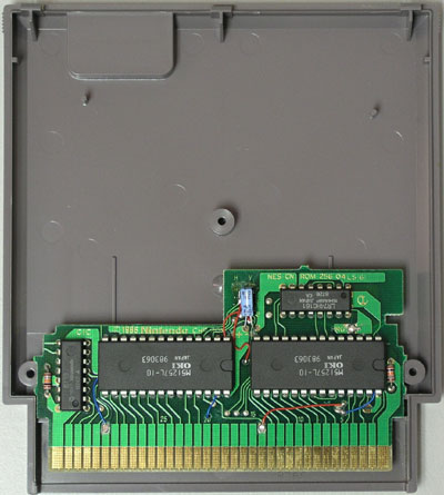
The topmost chip is the MMU. On the lower row, from left to right, are the CIC, the CHR-ROM, and the PRG-ROM chips.
Conclusion
The NES has many limitations compared to today's game consoles and personal computers. It has a limited CPU, a tiny amount of system RAM, a narrow data bus, and an idiosyncratic PPU. Despite this, it has an excellent library of games and it continues to be a much-loved console.
Changelog
- 2020-06-22 Initial version
- 2020-06-23 Minor formatting changes
- 2020-06-27 Minor formatting changes
- 2020-06-28 Minor formatting changes
- 2020-08-03 Minor wording changes
- 2020-08-26 Plain English improvements
- 2021-10-20 Rephrased the CRT scanning description
- 2024-04-11 Improved the zero page and PPU rendering descriptions
# Comments
Comments on this site are implemented using GitHub Issues. To add your comment, please add it to this GitHub Issue. It will then appear below.